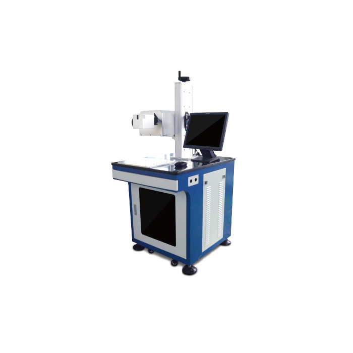
UV laser is suitable for cutting and marking on hardboard, rigid flex, soft board and the accessories. So what are the advantages of this laser?
The circuit board in SMT industry and micro-drilling holes in PCB industry, UV laser cutting system shows a great technical advantage. According to the different thickness of the board, the laser cuts the materials once or more times along the contour. The thinner the material is, the faster the cutting. If the accumulated laser pulse is lower than the laser pulse required penetrating the material, only scratches appear on the surface of the material; therefore, two-dimensional codes or bar code can be marked on the material for the tracking of the following processing.
Application of UV Laser Processing in PCB Industry
The pulse energy of the UV laser works on the material only a few microseconds and there is no significant thermal effect at a few microns next to the incision, so there is no need to consider the damage to the component due to the heat it generates. Close to the edge of the lines and solder joints intact, no glitches.
In addition, LPKF UV laser system can be integrated CAM software directly imported from the CAD derived data, edit with the laser cutting path, to form laser cutting contours, select the applicable parameter for different materials, you can directly choose laser processing. The laser system is not only suitable for large quantities production processing, but also for sample production.
Due to the short wavelength of UV laser, it can be applied to most of the material processing. For example, in the electronics industry can be used for:
Processing TCO / ITO glass and no damage to the substrate
Drill holes in flexible or thin materials
Solder mask or cover film window
Rigid soft/flexible circuit board sub-board
Slotted
Repaired or assembled without a circuit board
Cutting sintered ceramic
Precision Cutting LTCC


